An overview of microcontroller
Description
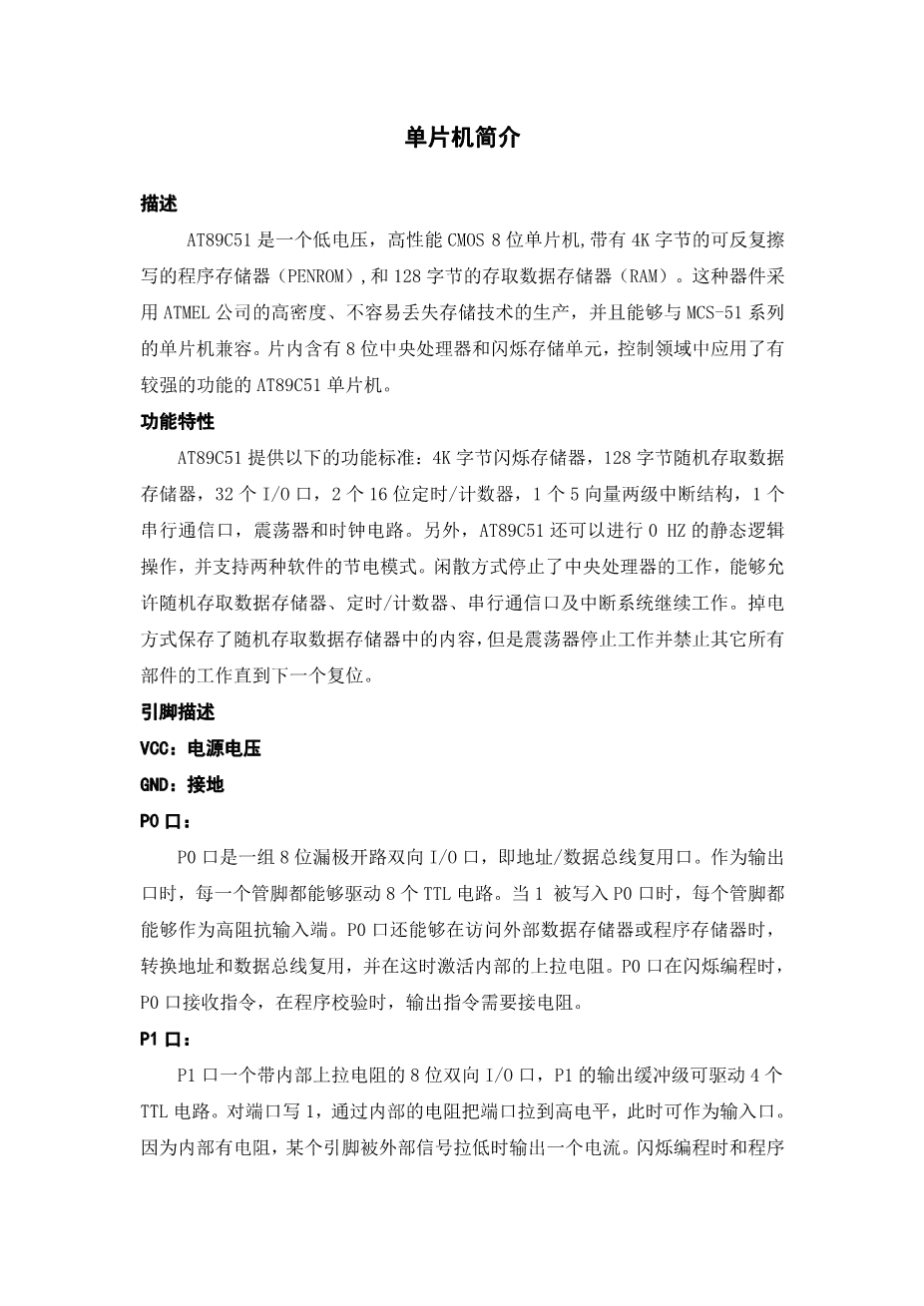
The AT89C51 is a low-power, high-performance CMOS 8-bit microcomputer with 4K bytes of Flash programmable and erasable read only memory (PEROM). The device is manufactured using Atmelrsquo;s high-density nonvolatile memory technology and is compatible with the industry-standard MCS-51 instruction set and pinout. The on-chip Flash allows the program memory to be reprogrammed in-system or by a conventional nonvolatile memory programmer. By combining a versatile 8-bit CPU with Flash on a monolithic chip, the Atmel AT89C51 is a powerful microcomputer which provides a highly-flexible and cost-effective solution to many embedded control applications.
Function characteristic
The AT89C51 provides the following standard features: 4K bytes of Flash, 128 bytes of RAM, 32 I/O lines, two 16-bit timer/counters, a five vector two-level interrupt architecture, a full duplex serial port, on-chip oscillator and clock circuitry. In addition, the AT89C51 is designed with static logic for operation down to zero frequency and supports two software selectable power saving modes. The Idle Mode stops the CPU while allowing the RAM, timer/counters, serial port and interrupt system to continue functioning. The Power-down Mode saves the RAM contents but freezes the oscillator disabling all other chip functions until the next hardware reset.
Pin Description
VCC:Supply voltage.
GND:Ground.
Port 0:
Port 0 is an 8-bit open-drain bi-directional I/O port.As an output port, each pin can sink eight TTL inputs. When 1s are written to port 0 pins, the pins can be used as highimpedance inputs.Port 0 may also be configured to be the multiplexed loworder address/data bus during accesses to external program and data memory. In this mode P0 has internal pullups.Port 0 also receives the code bytes during Flash programming,and outputs the code bytes during programverification. External pullups are required during programverification.
Port 1
Port 1 is an 8-bit bi-directional I/O port with internal pullups.The Port 1 output buffers can sink/source four TTL inputs.When 1s are written to Port 1 pins they are pulled high by the internal pullups and can be used as inputs. As inputs,Port 1 pins that are externally being pulled low will source current (IIL) because of the internal pullups.Port 1 also receives the low-order address bytes during Flash programming and verification.
Port 2
Port 2 is an 8-bit bi-directional I/O port with internal pullups.The Port 2 output buffers can sink/source four TTL inputs.When 1s are written to Port 2 pins they are pulled high by the internal pullups and can be used as inputs. As inputs,Port 2 pins that are externally being pulled low will source current, because of the internal pullups.Port 2 emits the high-order address byte during fetches from external program memory and during accesses to external data memory that use 16-bit addresses. In this application, it uses strong internal pullupswhen emitting 1s. During accesses to external data memory that use 8-bit addresses, Port 2 emits the contents of the P2 Special Function Register.Port 2 also receives the high-order address bits and some control signals during Flash programming and verification.
Port 3
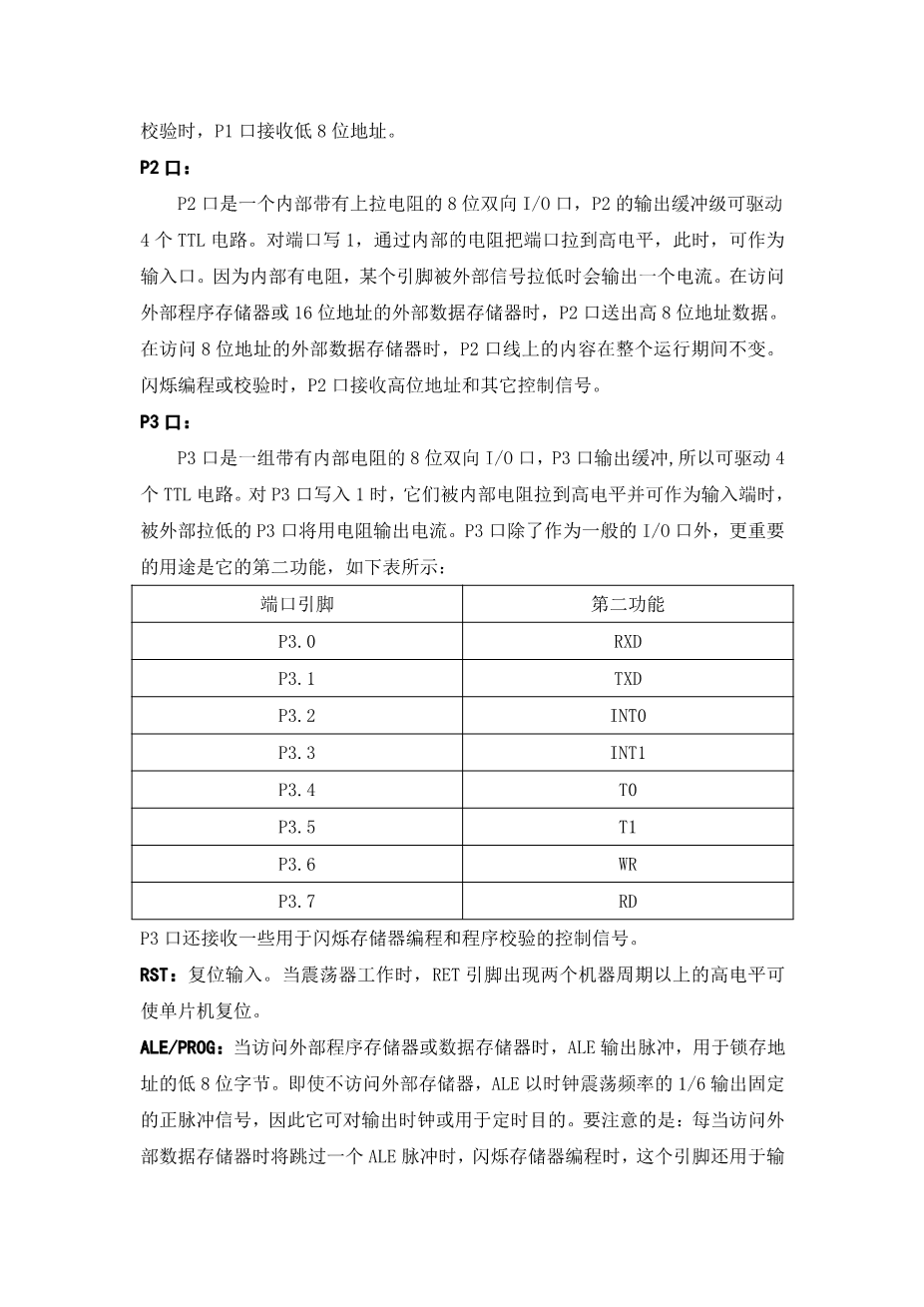
Port 3 is an 8-bit bi-directional I/O port with internal pullups.The Port 3 output buffers can sink/source four TTL inputs.When 1s are written to Port 3 pins they are pulled high by the internal pullups and can be used as inputs. As inputs,Port 3 pins that are externally being pulled low will source current (IIL) because of the pullups.Port 3 also serves the functions of various special features of the AT89C51 as listed below:
|
Port Pin |
Alternate Functions |
|
P3.0 |
RXD(serial input port) |
|
P3.1 |
TXD(serial output port) |
|
P3.2 |
INTO(external interrupt 0) |
|
P3.3 |
INT1(external interrupt 1) |
|
P3.4 |
T0 (timer 0external input) |
|
P3.5 |
T1(timer 1external input) |
|
P3.6 |
WR(external data memory write strobe) |
|
P3.7 |
RD(external data memory read strobe) |
Port 3 also receives some control signals for Flash programming and verification.
RST Reset input. A high on this pin for two machine cycles while the oscillator is runningresets the device.
ALE/PROG Address Latch Enable output pulse for latching the low byte of the address during accesses to external memory. This pin is also the program pulse input (PROG) during Flash programming.In normal operation ALE is emitted at a constant rate of 1/6 the oscillator frequency, and may be used for external timing or clocking purposes. Note, however, that one ALE pulse is skipped during each access to external Data Memory.
PSEN Program Store Enable is the read strobe to external program memory.When the AT89C51 is executing code from external program memory, PSEN is activated twice each machine cycle, except that two PSEN activations are skipped during each access to external data memory.
EA/VPP External Access Enable. EA must be strapped to GND in order to enable the device to fetch code from external program memory locations starting at 0000H up to FFFFH. Note, however, that if lock bit 1 is programmed, EA will be internally latched on reset.EA should be strapped to VCC for internal program executions.This pin also receives the 12-volt programming enable voltage(VPP) during Flash program
剩余内容已隐藏,支付完成后下载完整资料


英语译文共 11 页,剩余内容已隐藏,支付完成后下载完整资料
资料编号:[613580],资料为PDF文档或Word文档,PDF文档可免费转换为Word
课题毕业论文、开题报告、任务书、外文翻译、程序设计、图纸设计等资料可联系客服协助查找。
您可能感兴趣的文章
- 饮用水微生物群:一个全面的时空研究,以监测巴黎供水系统的水质外文翻译资料
- 步进电机控制和摩擦模型对复杂机械系统精确定位的影响外文翻译资料
- 具有温湿度控制的开式阴极PEM燃料电池性能的提升外文翻译资料
- 警报定时系统对驾驶员行为的影响:调查驾驶员信任的差异以及根据警报定时对警报的响应外文翻译资料
- 门禁系统的零知识认证解决方案外文翻译资料
- 车辆废气及室外环境中悬浮微粒中有机磷的含量—-个案研究外文翻译资料
- ZigBee协议对城市风力涡轮机的无线监控: 支持应用软件和传感器模块外文翻译资料
- ZigBee系统在医疗保健中提供位置信息和传感器数据传输的方案外文翻译资料
- 基于PLC的模糊控制器在污水处理系统中的应用外文翻译资料
- 光伏并联最大功率点跟踪系统独立应用程序外文翻译资料


